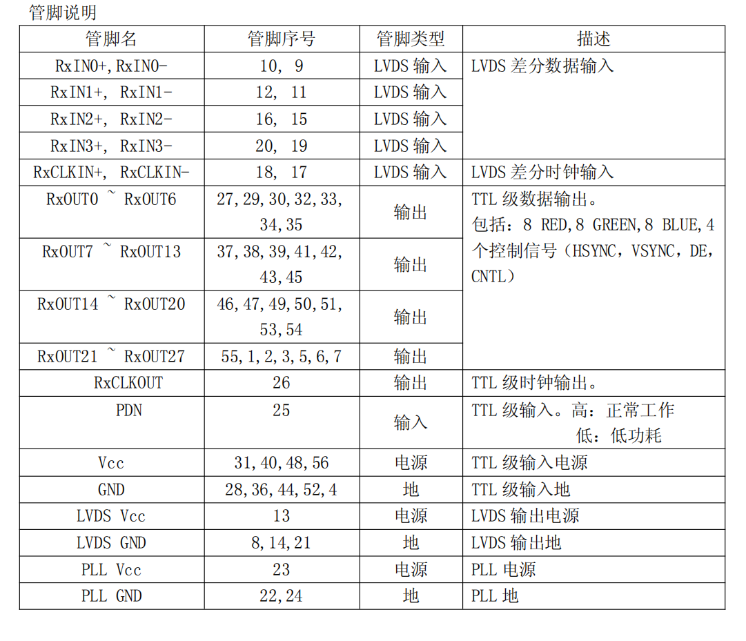
|
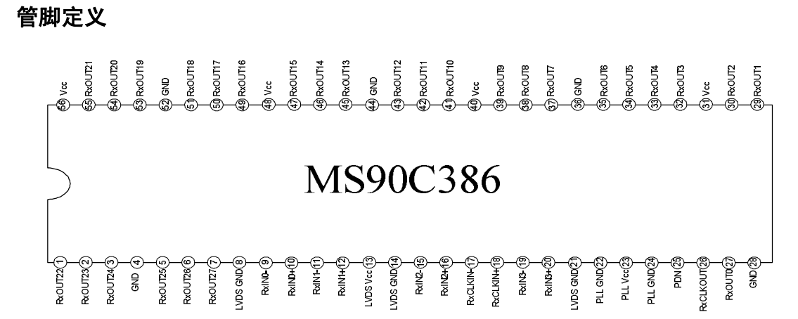
功能概述 MS90C386 芯片能够将 4 通道的低压差分信号(LVDS)转换成 28bit 的 TTL 数据。时钟通道与数据通道并行输入。在时钟频率为 175MHz 时,24bit 的 RGB 数据、3bit 的 LCD 时序数据和 1bit 的控制数据以 1225Mbps 的速率在每个 LVDS 数据通道中传输。输入时钟频率为175MHz 时,数据的传输速率为 612.5Mbytes/sec。此款芯片配合 MS90C385,是解决高带宽、高速 TTL 信号层面的电磁干扰和电缆长度问题的理想产品。 特点 频率范围:20-175MHz 时钟信号 较少的总线减少了连线尺寸和费用 供电电源 3.3V 低功耗模式 支持 VGA、SVGA、XGA、SXGA 4.90Gbps 数据吞吐量 612.5Megabytes/sec 带宽 减小 LVDS 摆幅来减小电磁干扰(300mVLVDS 摆幅) PLL 不需要外部结构 遵循 TIA/EIA-644LVDS 标准 TSSOP56 封装 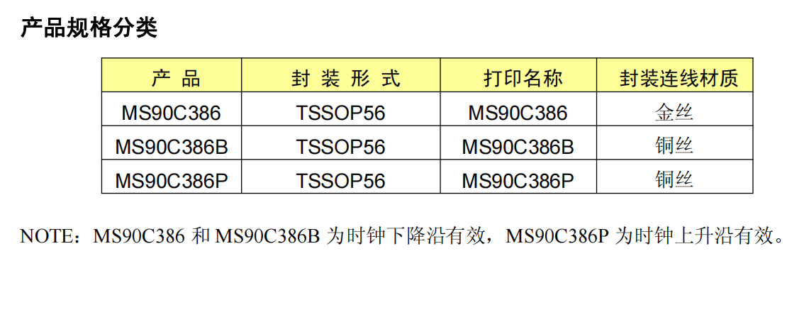
结构框图 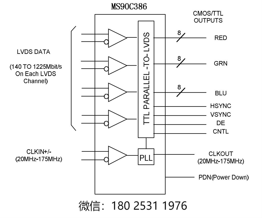
典型应用图 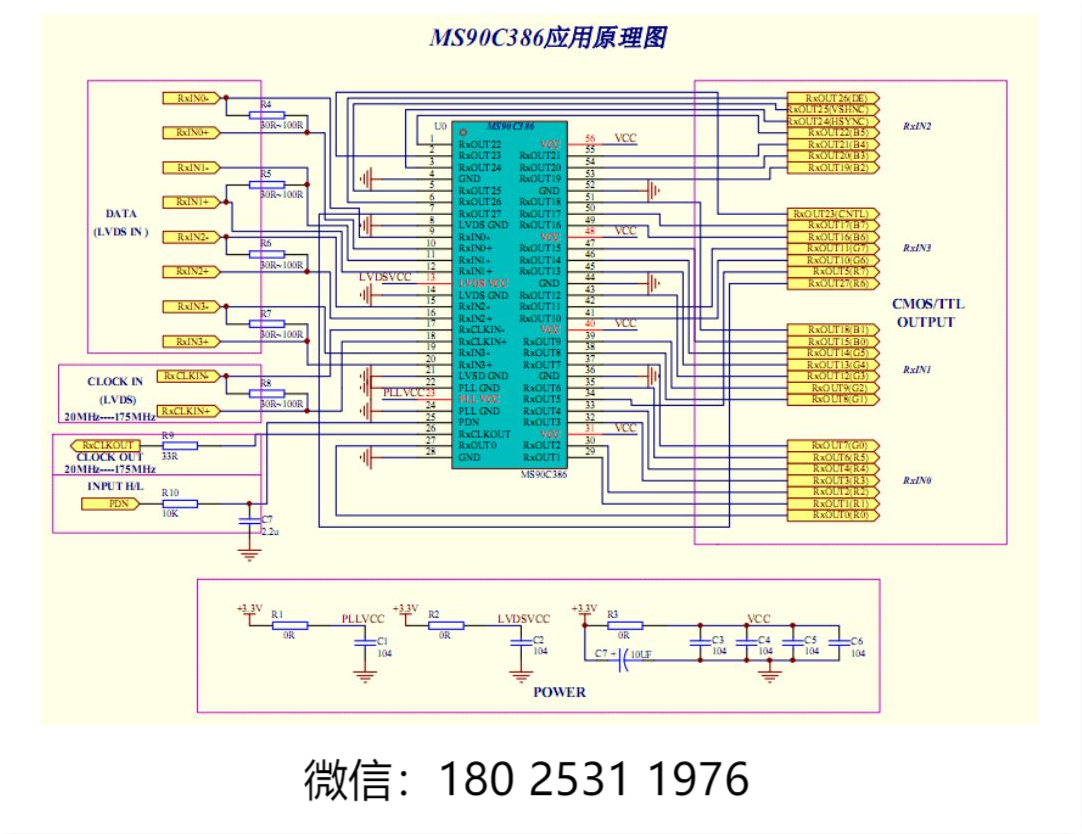
| 

 /1
/1 


 |手机版|OpenEdv-开源电子网
( 粤ICP备12000418号-1 )
|手机版|OpenEdv-开源电子网
( 粤ICP备12000418号-1 )


 发表于 2022-5-6 21:22:32
